Derzeit gibt es immer mehr Optionen für drahtlose SoC-Chips, von europäischen und amerikanischen Herstellern bis hin zu heimischen Halbleitern. Wie wählt man einen geeigneten drahtlosen Chip für die Produktentwicklung aus? Folgende Aspekte müssen berücksichtigt werden.
Kabellose Technologie:
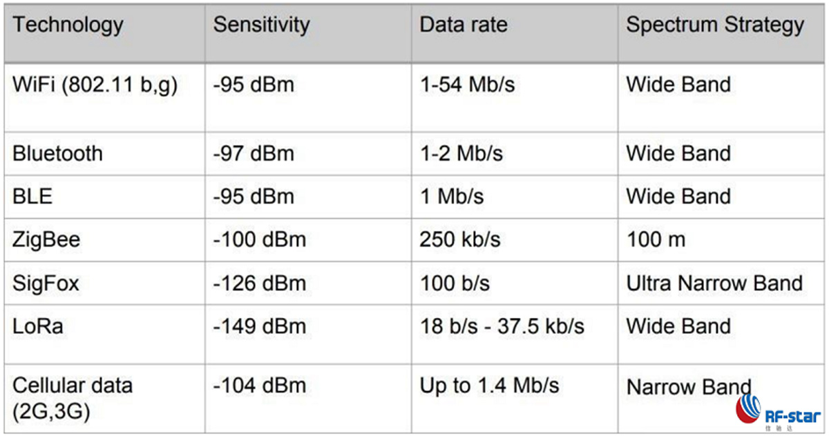
Zu den derzeit beliebten drahtlosen Technologien mit geringem Stromverbrauch gehören Wi-Fi, Small Wireless, LoRa, Bluetooth, Thread, ZigBee, NFC, Private 2.4G , NB-IoT, 2G, 3G, 4G usw. Die häufig verwendeten drahtlosen Technologien Fabrikautomation und Smart Home einschließlich Wi-Fi, Small Wireless, BLE , Thread, ZigBee, NFC. Die folgende Abbildung vergleicht die Vor- und Nachteile dieser verschiedenen drahtlosen Protokolle in Bezug auf Datenübertragungsbandbreite, Entfernung und Stromverbrauch. Je nach Nutzungsszenario sollte eine geeignete Lösung ausgewählt werden.

WLAN: WLAN eignet sich für die Hochgeschwindigkeitsübertragung von Videodaten, der Stromverbrauch ist jedoch relativ hoch. Derzeit gibt es auf dem Markt weniger Mainstream-Wi-Fi-Chips mit geringem Stromverbrauch. Der Kern verwendet einen ARM M3- oder M4-Kern, der ein einfaches RTOS ausführt und nur den 802.11b/g/n-Modus mit geringer Bandbreite unterstützt, aber die Anwendung einer Trockenbatterie-Stromversorgung erfüllen kann.
ZigBee: Die beste Wahl für Smart Home, der Status wird durch BLE MESH in Frage gestellt. Doch nach der Einführung von ZigBee 3.0 können verschiedene Systeme miteinander verbunden werden und die Kompatibilität der Plattform ist deutlich besser als zuvor.
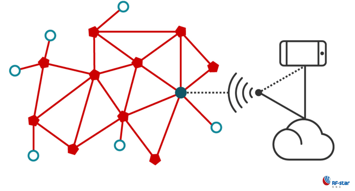
Sub-1G: Because of its stability and long transmission distance, it can be used in various industrial control fields. The TX peak current is large, but the system is in sleep mode at other times. Thus, the overall power consumption is low.
NFC: The function is which mobile phones must be carried with. Public transportation systems and access control systems are mostly adopted by RFID and NFC solutions.
LoRa: Unique spread spectrum technology, +20 dBm transmit power, low power consumption, long-distance, the disadvantage is low bandwidth utilization and low data throughput.
Power Consumption

Always keep the end users’ experience in mind. If the battery fails, even the most ideal product will be abandoned.
What kind of power supply method can be used? Coin cell, dry battery, lithium battery? Coin cells are popular due to their low cost, small size and lightweight. Considering that the battery life of these products is crucial, and the coin cell can only provide a peak current of about 5 mA without being damaged. If you drive a larger current peak, the battery capacity will be affected.
RF transmit power: The transmit power of Bluetooth is restively low. Usually, only 5 dBm transmit power is supported, generally refer to 0 dBm transmit power according to specifications. ZigBee, small wireless transmission power can reach 20 dBm. (More than 20 dBm cannot pass the safety test).
MCU operating power consumption: Because the same ARM core of the wireless SoC is used, the power consumption is similar to each other. But it is necessary to evaluate the MCU running time from wakes up status from low power mode to full speed operation. The longer the time, the greater the power consumption. In addition, it is necessary to evaluate the MCU main frequency at full speed. The higher the main frequency, the greater the power consumption.
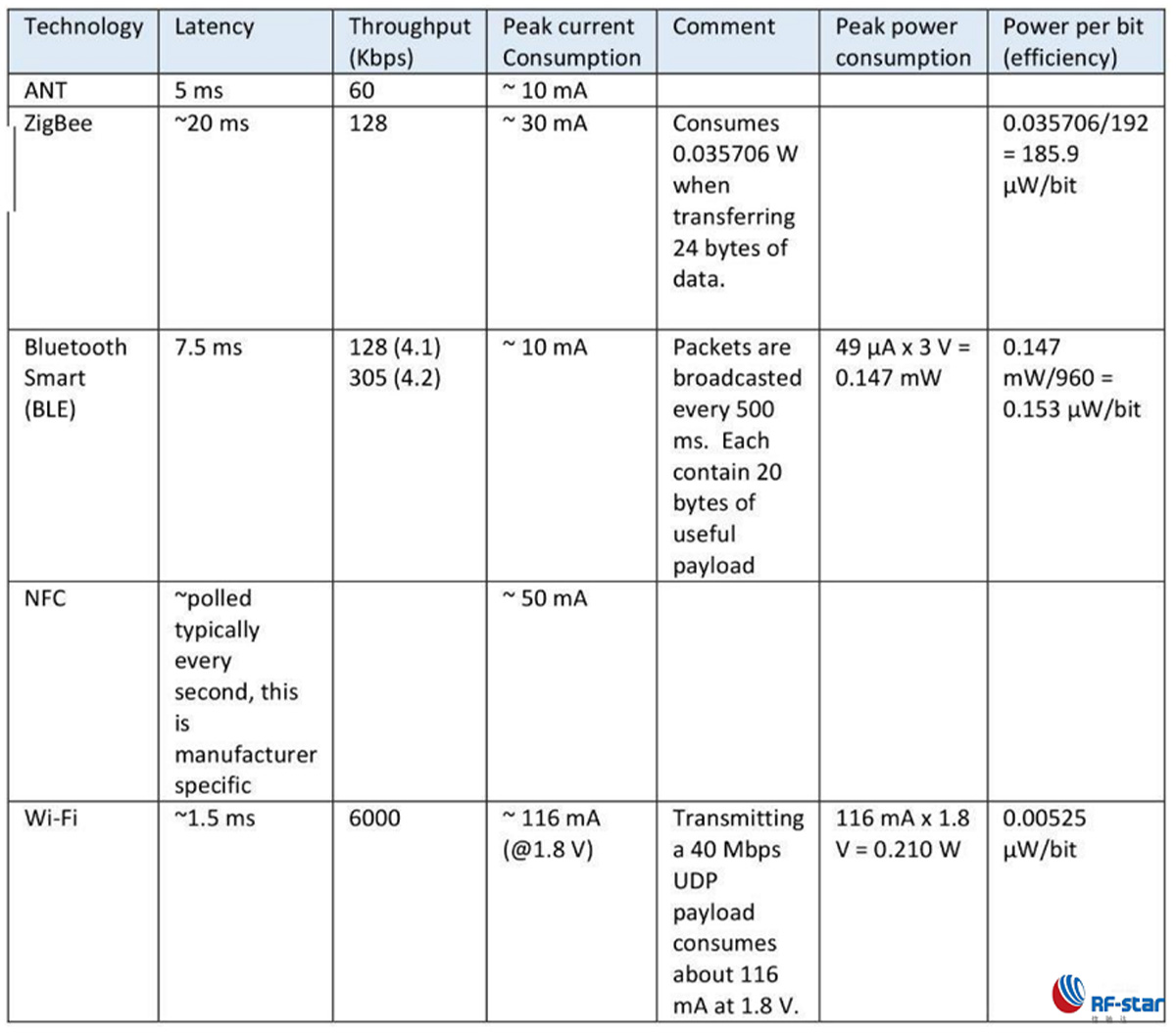
The following figure shows the power consumption performance of several IoT technologies:
In addition to the specifications, several suggestions for reducing power consumption are provided:
1.Adjust the connection interval, advertising interval and slave delay accordingly.
2.Combine multiple small data packets into fewer large data packets to reduce RF overhead.
3.Consider compressing data locally before transmission to reduce RF throughput.
4.Identify non-critical data that can be sent or not be sent at a slower rate.
Memory Selection

Main indicators of memory: RAM, FLASH, ROM, serial FLASH
RAM: The temporary variables, global variables, arrays, etc. applied in the code are all placed in RAM. The size of RAM will determine the complexity of the system. Early devices such as CC2541 and nRF51822 have fewer RAM resources, which will limit the number of BLE connections as a master, and will also affect the execution efficiency of the algorithm (usually a real-time algorithm will load the code from flash to RAM to run).
Usually need to consider RAM space greater than 20K. (Because RTOS and protocol will also take up some RAM space).
FLASH: The key factor determines the program. Usually Flash requires more than 256K, and the commonly used one is between 256K ~ 512K. Some manufacturers, such as the 1M flash launched by nRF52840, are slightly larger and maybe the products developed for wearable devices.
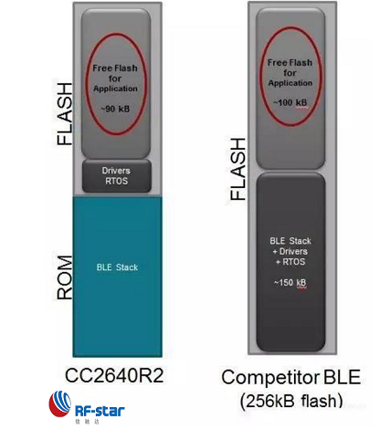
ROM: You may have the question why is ROM mentioned here? Because the cost of ROM is low, some manufacturers such as Dialog, TI and other manufacturers will put the protocol stack in the ROM to reduce the cost of chip manufacturing. For example, TI's public information is as follows :
Serial FLASH: This is more interesting. If IoT market managers look at domestic and overseas wireless chips, they can find the interesting point. Overseas semiconductors will integrate flash into the chip. Domestic semiconductors integrate serial flash into the chip or external flash. The reason is all because of the cost! Serial flash is cheap. Using a large-capacity RAM to load the program from the serial flash to the RAM is much lower than the cost of running directly on the on-chip flash. (XCODER has a suggestion here. It is recommended to consider digitally signing and encrypting the firmware stored in the off-chip flash in the chip ROM. Otherwise, it is easy for the pirates to read the firmware from the flash of the customer's product and then copy the product in reverse.)
OTA Upgrade

IoT's products are in a period of rapid iteration. It doesn't mean the product iteration is fast, but that the software updates quickly, including bugs, the interactive interface update, the control logic update, etc. All these can't expect to recycle the products and then disassemble them. We must consider the functional requirements of wireless OTA upgrade and leave a way to upgrate for our products.
Here's how to control the demand for OTA upgrade:
Air rate during upgrade:
The speed determines the user’s experience of the upgrade. The longer the air transmission time, the greater the probability of problems. Therefore, it is the most difficult to use LoRa to do air upgrades.
Memory flash capacity:
Over-the-air upgrade can be divided into two upgrade methods. First, the image backup upgrade requires twice the storage space of the firmware. The new backup file first receives and stores into the flash, and the boot program is used to run the new firmware after restarting. Second, there is no image upgrade. After entering the upgrade mode, directly erase the firmware in the flash memory and write the new firmware. This upgrade mode requires the boot program to support the OTA function, which can avoid the product becoming bricks caused by the upgrade failure.
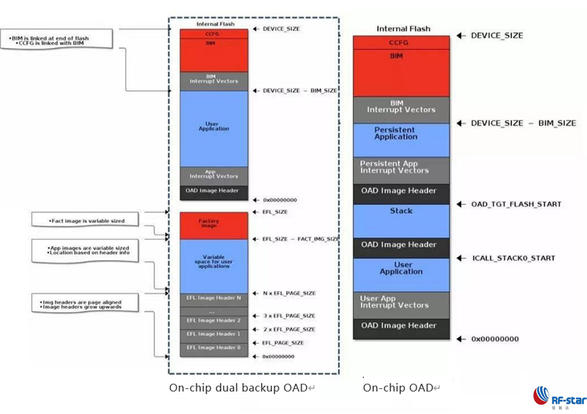
Therefore, the capacity of flash is also an aspect that needs to be evaluated. Don't blindly reduce the cost and reduce the flash size. It is suggested that the flash capacity should be 1.5 to 2 times the flash size of its own application layer.

Multi-protocol integration
The current product applications use both Bluetooth and small wireless. Of course, multi-chips can be used for integration. However, there are already manufacturers on the market that have achieved multi-protocol integration by binding wafers from different original manufacturers. One chip solves multiple protocols. I think this is a transitional product. Because of the internal multiple wafers and multiple MCUs running at the same time, power management is a big challenge.
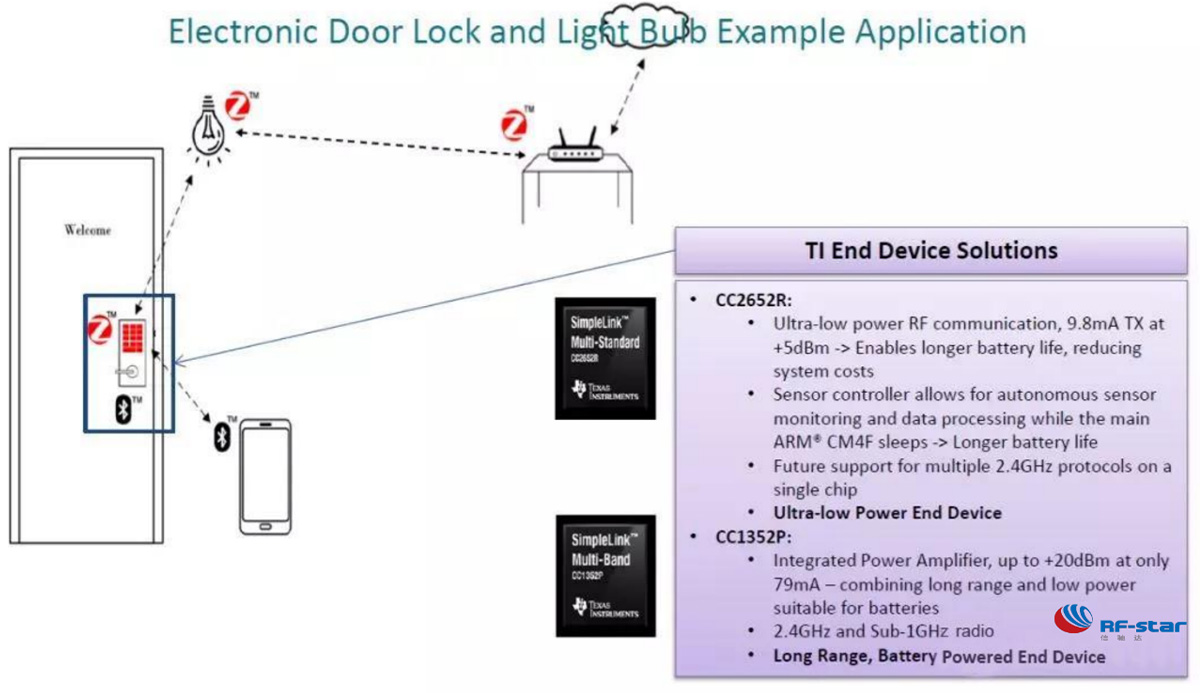
At present, European and American semiconductor manufacturers are already deploying multi-protocol integration, starting from the chip design, combining 2.4G and small wireless on a single SoC chip, and completing the multi-protocol functions through software time-division multiplexing. I believe this is a trend in the foreseeable future. It can be considered when multi-protocol collaborative applications are required. According to the official announcement of Texas Instruments, the CC1352 and CC2652 chips already support this function, and the technology has been applied to smart door lock applications.
